KP Technology leads the way in enabling researchers to improve the characterisation of their materials.
Our expertise supports the development of emerging and cutting-edge materials technology.
Current exciting growth areas include, solar cells, perovskites, 2D materials, graphene, OLEDs, photovoltaics and Molybdenum research, however this technology can be applied to many scientific fields.
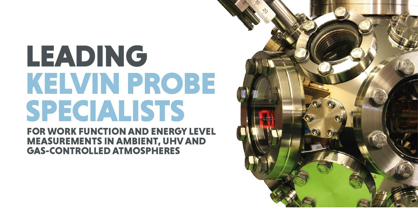
Our most popular systems feature surface photovoltage (SPS) and photoemission spectroscopy capabilities to determine the absolute work function in ambient, controlled gas or vacuum environments.
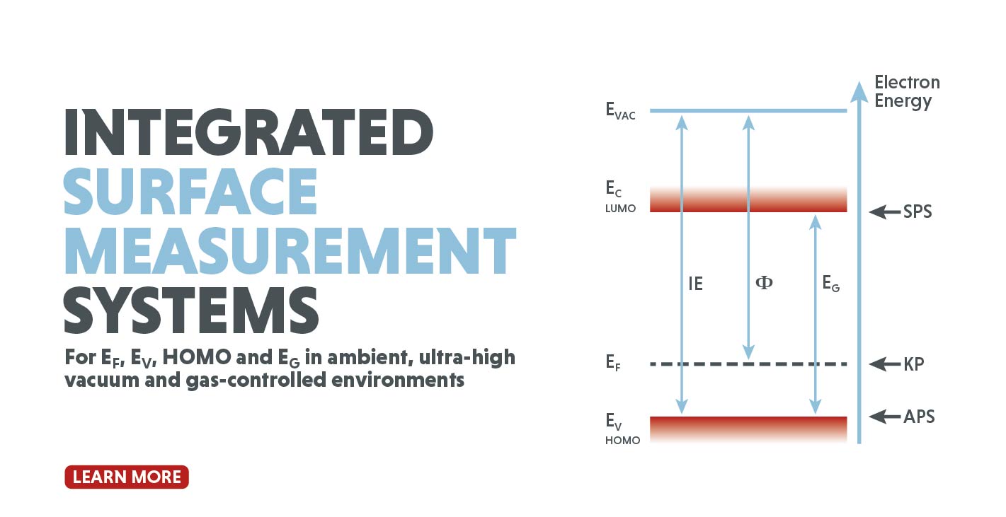
Knowledge of the electronic properties occurring in semiconductor materials is central to understanding light absorbing devices such as solar cells and light emitters such as LEDs. The relevant energy levels presented in the Energy Band diagram show the partially filled and unfilled electron energy bands against a vertical energy axis, with the zero energy, or Vacuum Level at the top.
Semiconductors are characterised by two electron bands: the “Valence Band” (or in organic semiconductors the HOMO level) which is fully occupied by electrons up to energy EV and the upper “Conduction Band” (LUMO) which is partially populated from energy level EC. The semiconductor fermi-level EF is normally determined by the semiconductor bulk doping but can be influenced by illumination.
Under dark conditions the vibrating Kelvin Probe (KP) provides the fermi-level EF, and with spectroscopic illumination (KP-SPS) energy EC can be determined. Ambient Pressure Photoemission spectroscopy (APS) provides EV.
Find out more about Air Photoemission here or view the Ambient Pressure Photoemission Spectroscopy product range.


We are impressed with the performance of the custom built APS04 system from KP Technology. This equipment provides an accessible method to measure important energy levels in layers and complete devices. I am happy with all aspects of the technical support provided by company director Prof. Baikie and his staff.
Professor Arie Zaban, President, Bar-Ilan University
We find KP Technology’s Ambient Pressure Photoemission System/APS04 extremely useful for determining the energy levels of OLED and solar cell materials.
Professor Ifor Samuel, Dean of Research, University of St Andrews
The Kelvin probe system from KP Technology functions as the corner-stone for us to investigate the work function of our organic/inorganic materials which subsequently influence performances of the optoelectronic devices. The team members learn a lot from the comprehensive support of KP Technology on using the system and analyse the data.
Professor Wallace Choy, University of Hong Kong
I appreciate your consideration and time invested in answering any questions. Our Kelvin Probe has become a good friend and is an amazing machine. I cannot praise the work it has done for us enough.
Dustin Rasmuson, Materials Scientist